Search...



Description:
The UCC21530-Q1 is an isolated dual-channel gatedriver with 4A source and 6A sink peak current. Itis designed to drive IGBTs, Si MOSFETs, and SiCMOSFETs up to 5MHz.The input side is isolated from the two outputdrivers by a 5.7kVRMS reinforced isolation barrier,with a minimum of 125V/ns common-mode transientimmunity (CMTI). Internal functional isolation betweenthe two secondary-side drivers allows a workingvoltage of up to 1850V.This device can be configured as two low-side drivers,two high-side drivers, or a half-bridge driver withprogrammable dead time (DT). The EN pin pulled lowshuts down both outputs simultaneously and allowsfor normal operation when left open or pulled high. Asa fail-safe measure, primary-side logic failures forceboth outputs low.The device accepts VDD supply voltages up to 25V.A wide input VCCI range from 3V to 18V makes thedriver suitable for interfacing with both analog anddigital controllers. All the supply voltage pins haveunder voltage lock-out (UVLO) protection.
Features:
• AEC-Q100 qualified with:– Device temperature grade 1
• Functional Safety Quality-Managed– Documentation available to aid functional safetysystem design
• Universal: dual low-side, dual high-side or halfbridge driver
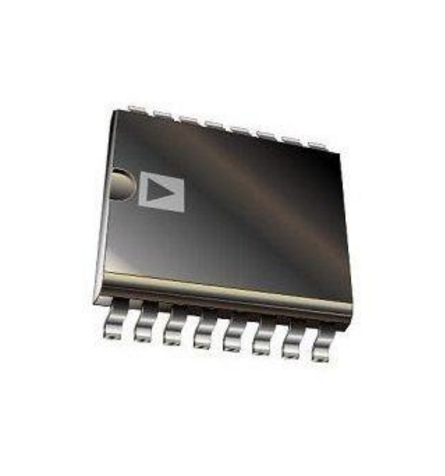
• Wide body SOIC-14 (DWK) package
• 3.3mm spacing between driver channels
• Switching parameters:
– 33ns typical propagation delay
– 20ns minimum pulse width
– 6ns maximum pulse-width distortion
• Common-mode transient immunity (CMTI) greaterthan 125V/ns
• 4A peak source, 6A peak sink output
• TTL and CMOS compatible inputs
• 3V to 18V input VCCI range
• Up to 25V VDD output drive supply
– 8V,12V and 17V VDD UVLO options
• Programmable overlap and dead time
• Junction temperature range –40 to +150°C
Applications:
• HEV and BEV battery chargers
• Solar string and central inverters
• AC-to-DC and DC-to-DC charging piles
• AC inverter and servo drive
• AC-to-DC and DC-to-DC power delivery
• Energy storage systems
You can get your TI UCC21530QDWKRQ1 Datesheet solution by flling out the form below and we will contact you immediately.
AXTEK Series NYQUEST CMSEMICON ST MICROELECTRONICS Featured Manufacturers Puya MCUs ICMAN Touch Chips ZXInfoTek Holtek MCUs MORNSUN Modules
Company Profile Certificates Terms & Conditions Privacy Statement


 MCU Solutions
 PCBA Solutions
 Bluetooth Solutions

 FAQ
 Contact Us

 Company News
 Technology News
 Industry News
 PCBA News

 Company Profile
 Certificates
 Terms & Conditions
 Privacy Statement

 Home Appliances
 Beauty Appliances
 Lighting
 Kid's Toys
 Security Alarm
 Health Care